

Dual-speed PLL designed for wideband FM transmitter.
Power supply: 8-15 V stabilized, 40 mA
Frequency range: 82,5-108 MHz
Step frequency: 100 kHz
RF input voltage range: 10-500 mV
RF input impedance: 135 ohm
Schematic diagram:
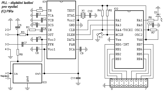
Pin meaning:
1 - tuning voltage (output)
3 - RF signal from oscillator (input)
2, 4 - ground
Tl1 - reset
Daftar Komponen:
Capacitors:
C1, C12 - 2,2 nF (ceramic)
C2, C9 - 10 nF (ceramic)
C3 - 47 uF (electrolytic)
C4 - 10 uF (tantalum)
C5 - 0,47 uF (electrolytic)
C6, C11 - 100 nF (ceramic)
C7 - 1 nF (ceramic)
C8 - 220 uF (electrolytic)
C10 - 22 pF (ceramic)
Resistors:
R1 - 1k
R2 - 4k7
R3, R4, R5, R7 - 10k
R6 - 1k (optional)
R8 - 47k (optional, see below)
Misc.:
IC1 - SAA1057
IC2 - PIC16F84 (programmed) + socket
IC3 - 78L05
X1 - 4 MHz crystal
D1 - LED diode (optional)
Tl1 - button (optional)
jumpers or DIP switches
Software for the IC2:
pll16f84.asm, pll16f84.hex. Oscillator type: RC, watchdog: ON.
Jumpers/DIP switches setting: see pllfreq.txt or download user-friendly program!
Instructions
Para TL1 tombol reset unit. Tekan setelah mengatur frekuensi. Unit ini menyediakan reset pada kekuasaan-up, sehingga Anda tidak perlu menggunakan tombol.
D1 LED menunjukkan siklus tuning dilakukan (setelah satu detik dari reset). Ini tidak diperlukan untuk menggunakannya dan resistor R6.
Resistor R8 menyediakan tegangan minimal sekitar 2 V pada output PLL. Gunakan resistor ini jika transmitter osilator tidak bekerja jika tegangan tunning di bawah nilai ini (terutama setelah power-up). Tempatkan resistor di R3.
Catatan.
- Output of the PLL should not be directly loaded with big capacities (over about 0,3 uF). The PLL loop may be unstable. This applies to some unknown transmitters.
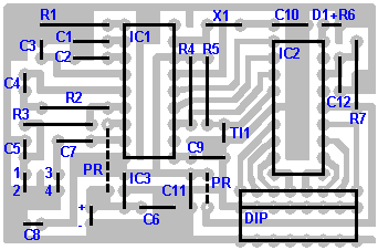
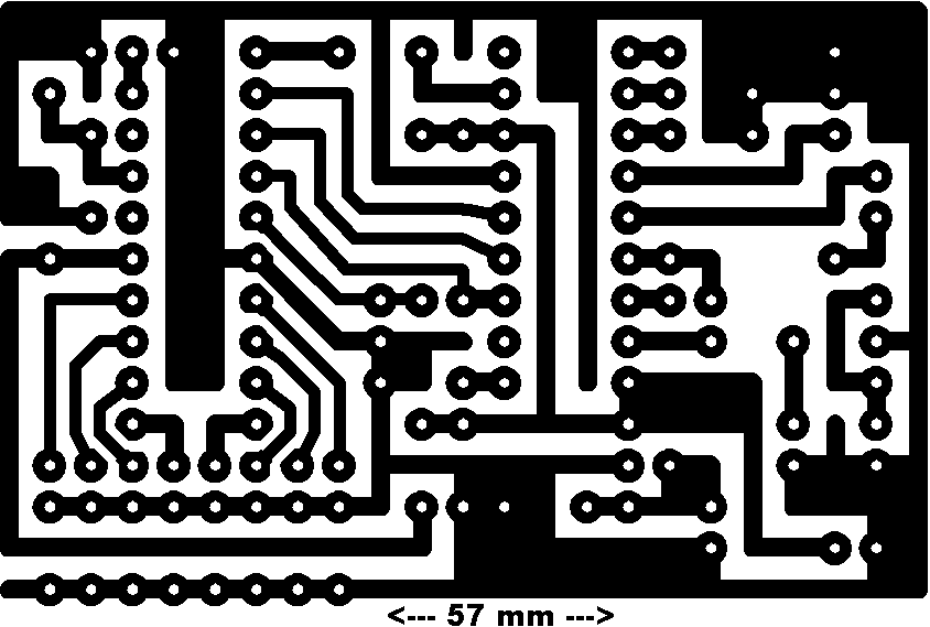
PCB layout
[Joko-Electronic]
Subscribe by Email
Follow Updates Articles from This Blog via Email
No Comments