Jumat, 26 Agustus 2011

thumbnail

Oprek SoundCard Usb PCM2704


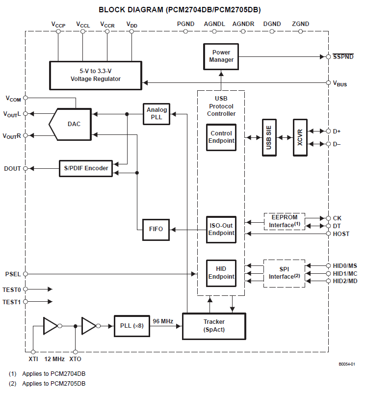
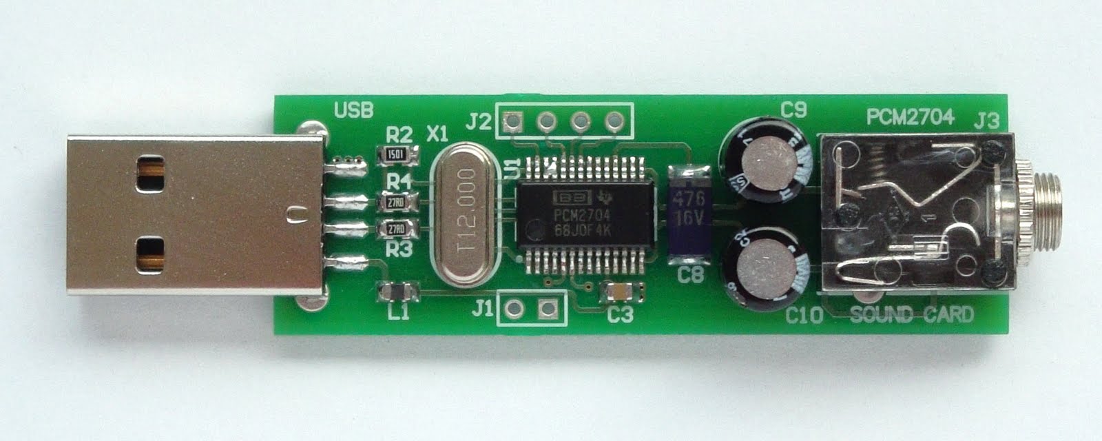
Perangkat ini penuh kartu suara fungsional untuk PC. Keuntungan utama menggunakan PCM2704 terhadap PCM2702 adalah konstruksi jauh lebih mudah. Seperti yang dapat Anda lihat pada diagram blok itu memiliki built-in 5V dan 3,3 regulator tegangan, HID antarmuka (MUTE, VOL +, VOL-), S / PDIF output. Sirkuit dapat diaktifkan langsung dari port USB. Keuntungan berikutnya adalah bahwa output DAC dapat drive langsung 32ohms headphone.

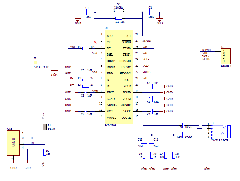
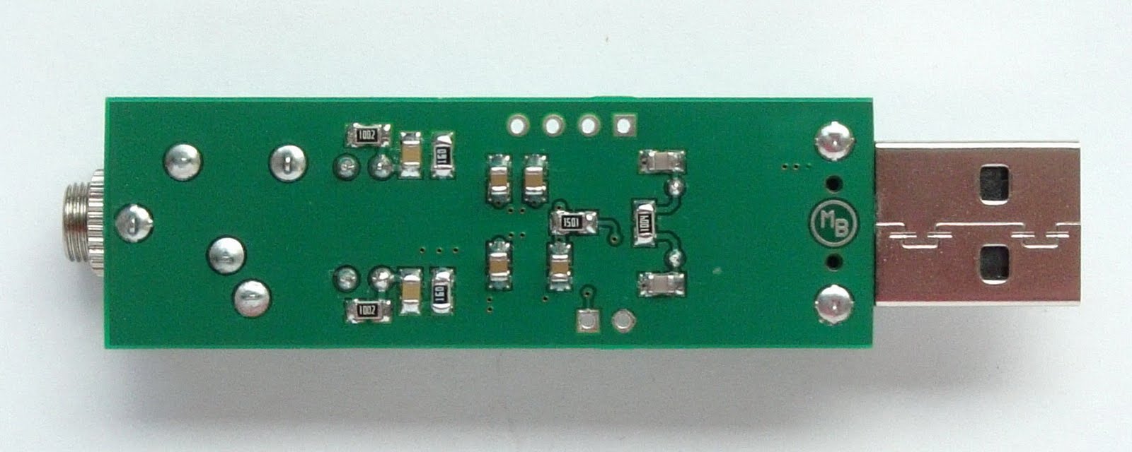
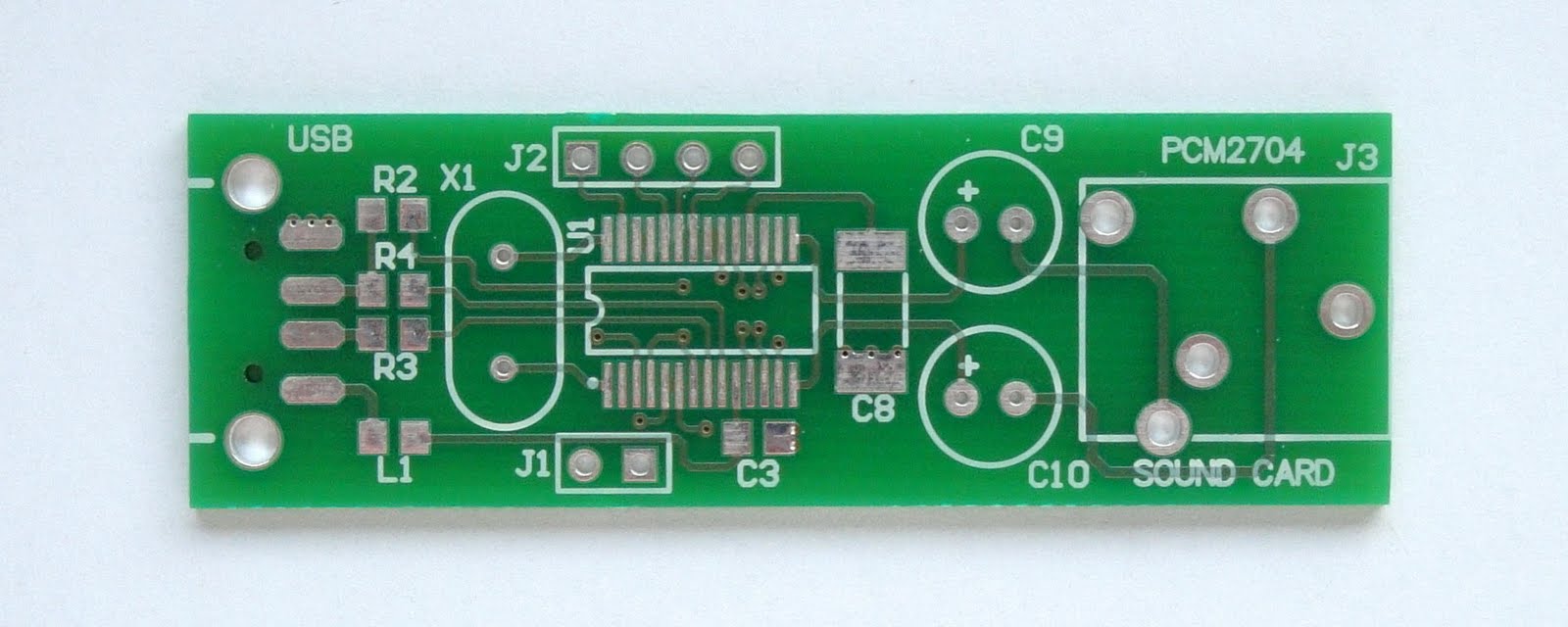
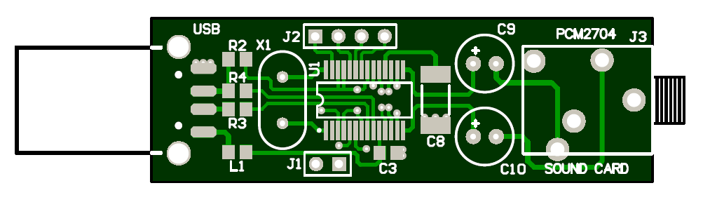
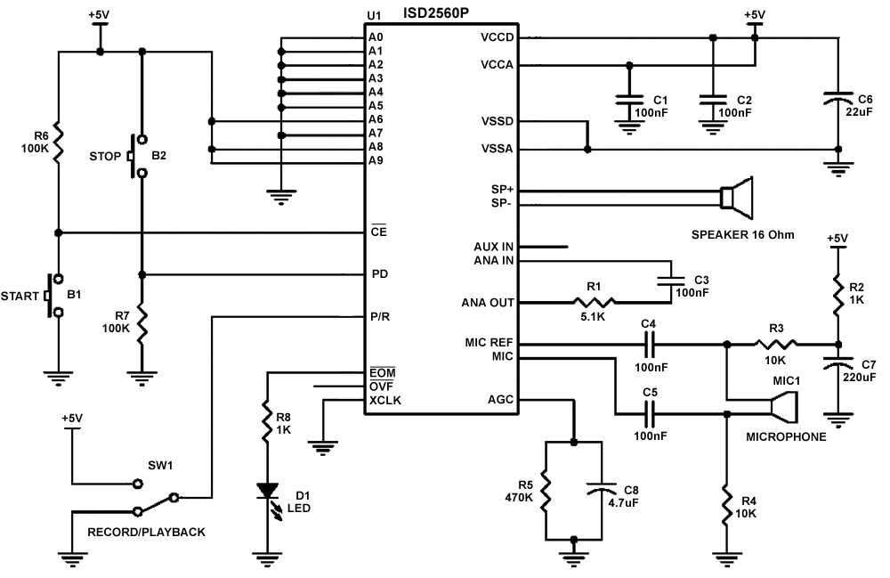
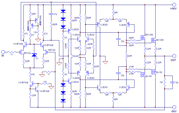
Skema sangat sederhana. Hal ini hampir salinan dari diagram sirkuit datasheet. Anda dapat melihat inti IC PCM2704 (U1), kristal dengan bagian-bagian pendukung (X1, C1, C2, R1), koneksi ke USB (USB, R2, R3, R4, L1), banyak kapasitor untuk memblokir semua tegangan (C3, C4, C5, C6, C7, C8), S / PDIF output header (J1), HID header (J2), filter output (R5, C11, R6, C12, R7, R8), kopling kapasitor (C9, C10) dan output konektor 3.5mm Jack (J3).

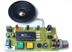
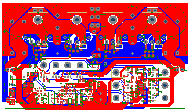
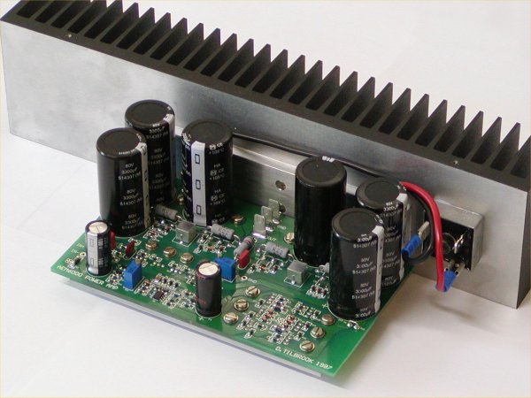
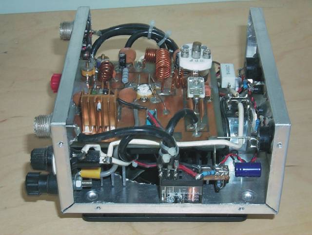
Saya merancang saya PCB sendiri. Dimensi dari PCB 55x18mm, termasuk USB dan Jack konektor itu adalah 73x18mm. Untuk menjaga ukuran sekecil mungkin 0805 ukuran kapasitor dan resistor digunakan. L1 adalah manik ferit yang mengurangi dengungan frekuensi tinggi. Dengan besi solder yang baik dan pengalaman litle adalah mungkin untuk perakitan PCB dengan tangan.

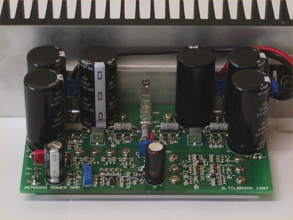
Saya membangun dua buah kartu suara. Saya telah menguji kartu suara di bawah Windows XP dan Windows Vista dan bekerja tanpa masalah apapun. Saya ingin menggunakan perangkat ini untuk penerima radio internet saya, yang saya sedang membangun sesuai dengan proyek yang diterbitkan pada mightyOhm.com. Penerima ini didasarkan pada Asus WiFi router WL-520GU dengan distribusi Linux OpenWRT. Kartu suara bekerja di bawah Linux juga, tapi berhenti dan mulai bermain suara periodik (periode bervariasi dari beberapa menit sampai satu jam). Saya kira itu adalah masalah driver (jika seseorang memiliki ide bagaimana untuk memperbaikinya saya akan sangat berterima kasih).

Anda dapat bertanya kepada saya mengapa untuk membangun kartu suara ketika Anda dapat membeli perangkat yang sama untuk beberapa dolar. Saya juga satu kartu suara dari Cina yang biaya sekitar 5 $ tapi kualitas suara sangat buruk, sehingga perbedaan utama adalah kualitas suara.


thumbnail

Digital Voice Recorder ISD2560

Proyek ini didasarkan pada ISD2560P IC yang memungkinkan kita untuk merekam suara 60 detik dan pemutaran dengan kualitas yang sangat tinggi. Seperti ditunjukkan dalam skema, kita masukan suara dengan menggunakan mikrofon electret. Jika mikrofon dinamis digunakan, R2, R3, R4 resistor dan C3, C5, C7 kapasitor akan dihilangkan dan mikrofon akan terhubung ke 17 dan 18 pin nomor secara langsung. Karena memiliki respon frekuensi yang lebih baik, kita memilih mikrofon electret dalam proyek ini.


thumbnail

Memecah Bagan 100W HiFi MOSFET Amp


The neat thing about the series 5000 is that it was built around new (at the time) Hitachi lateral power MOSFETs. Most power MOSFETs (VMOS, trenchFETs, HexFETs etc) use a vertical structure, where the current flows vertically. This has the advantage of stunningly low Rds and hence high efficiency, but does nothing for linearity or capacitance. Lateral MOSFETs are a much simpler structure, where the gate oxide is formed on a flat substrate, and the current flows across the substrate. This results in well defined, controllable device parameters, good linearity, and relatively low gate capacitance. However, the Rds of lateral MOSFETs is nothing to write home about.

MOSFETs also have a high input impedance at low frequencies, and are capable (when driven by a suitable source) of extremely high slew-rates. Of course this very attribute makes them rather prone to HF oscillation when improperly compensated, but with careful design they're capable of impressive intermod performance.


thumbnail

Bikin Stereo HeadPhone Sendiri

nah kawan kawan pengemar electronic yang suka ber experiment nah ini saya ada sebuah experiment kecil yang bisa anda buat sendiri yaitu buat mini power buat headset atau bahasa keren nya power headphone heheh sama aja ya namanya :) oya kawan berikut ini scemanya buat agan agan sekalian


sceman di atas mengunkan 3 buat transistor power dengan mode otl tipe tr bisa nada modif juga kok berikut daftar komponennya
R1 - 100K
R2 - 330
R3 - 100
R4 - 22 (2 - 4.5V)
R4 - 100 (5 - 12V)
C1 - 4.7uF
C2 - 4.7uF
C3 - 100 - 1000uF
C4 - 220uF

P1 - 100K
D1, D2 - 1N4148
Q1, Q2 - BC549/9014
Q3 - BC559/9012
Technical Specifications:
Supply Voltage: 2 - 12V
Energy Consumption: 10mA/3V - 30mA/12V
(measurements taken using a stereo version)
Output Power: 300mW

thumbnail

30 Watt Linear FM Amp with BLY89

A amplifier of medium force RF for the FM, is always essential for the amateur that wants it strengthens some small transmitter, that likely it has already it manufactured! The present circuit can give force 25-30W, with control no bigger than 4-5 W. As it appears in the analytic drawing, the amplifier is manufactured with the transistor TR1 of type LY89 of Phillips. The transistor this is specifically drawn for operation in frequencies up to 175Mhz, with very good results.

His special characteristics appear below:

Tendency of operation: 18V
Current of Collector: max 3 5th
Gain: max 10dB
Force of Expense: 25-30 W
Output (order C): > 60%

Variable capacitors C1, C2, with inductor L1, constitute the coordinated circuit that adapts the exit of our transmitter in this amplifier RF. the circuit has been calculated suitably, so that it covers all band the FM with the biggest possible output. Inductor RFC1 polarize the transistor, so as to it works in order C that is to say with the biggest output. Inductor L2 in the collector of TR1, constitutes the charge of amplifier, while RFC2 prevents the RF signals escape in the line of catering. Capacitor C2 and resistance R1, protect the circuit from auto polarize.

The coordinated circuit of expense that is constituted by inductor L2 and variable capacitors C3, C4, adapts the exit of amplifier RF with the next stage that can be some amplifier RF of high force (> 100W) or a aerial.

MANUFACTURE

The manufacture of amplifier is very simple and easy. Puncture the point PCB that will pass the nutshell of TR1. Stick the capacitors, variable, the resistance, the RF tsok and the inductors. Finally you stick the TR1, being careful not overheats at the welding and blend pin his. Clean finally PCB from the residues of soldering. Make a very careful control for by any chance errors, omissions, short-circuits, chills you stick also anything other that could you make wonder why does not work the amplifier.

PARTS

C1, C2, C3, C4 = 10 -80pF

C 5 = 10nF

C6 = 1000pF

C7 = 100nF

C8 = 2200mF/35V

L1 = 1 coil with diameter of 10 mms, 1 mm

L2 = 7 coils with diameter of 10 mms, 0,8 mm

L3 = 3 coils with diameter of 10 mms, 1 mm

TR1 = BLY89

RFC = RF tsok

If all they are it includes, you connect the exit of your transmitter (3-4W) in the entry of amplifier. The exit of amplifier him you will connect in some charge (dummy load) or in the aerial, through a bridge stagnant. Be supplied with tendency 11-15V your amplifier. (Power supply it should it provides current 45th). Regulate the 4 variable (C1-C4, until you take the biggest force of expense. The amplifier is ready.
thumbnail

Power Rf Amplifier 100Watt 2sc2782

Dengan Daya Input 10 Watt mampu mengeluarkan Daya 100Watt dengan penguatan akumulasi 10 Db wah bisa mamancarakan buat jarak jauh nih berikut ini sekematic nya


RF Power Amplifier Schematic and PCB

[RF Power Amplifier 2SC2782 50 MHz Left] [RF Power Amplifier 2SC2782 88 MHz Right]

RF Amplifier features:

Input Power: 10W
Output Power: 100W
Operating Frequency: 88-108MHz
Operating Mode: FM- SSB
Operating Voltage: 10-16V DC
Operating Current: 12A DC for 100W RF output
TX trigger:

Trigger by internal RF power input detection circuit.
Trigger by external equipment trigger output.


About