Safety Instructions
Caution mortal danger: The following circuit operates at a mains voltage of 230 Vac. Because of rectification, some of the components carry dc voltages of more than 322 V. The circuit should be disconnected from the mains and de-energized before any work is attempted on it. Note that capacitors located on the primary side will be charged with high voltage for several seconds even after switching of the mains voltage.
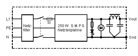
Experiments with the PC power supply encouraged me to produce an "improved" design. Like the original design, the new power supply is also a forward converter with a half-bridge topology. The differences to the modified PC power supply consist of the following items: 1) two power FETs are used instead of bipolar transistors as power switches, 2) a synchronous rectifier on the secondary side instead of power diodes, 3) the elimination of a switch driver stage (current-proportional control), and 4) a simpler over-current and over-voltage monitor. With the magnetic components (output transformer, driver transformer, chokes...) stripped from a PC power supply, the new power supply delivers a max. power output of 250 W with efficiency up to 90 %. The power supply can handle 20 % overload for a short duration.
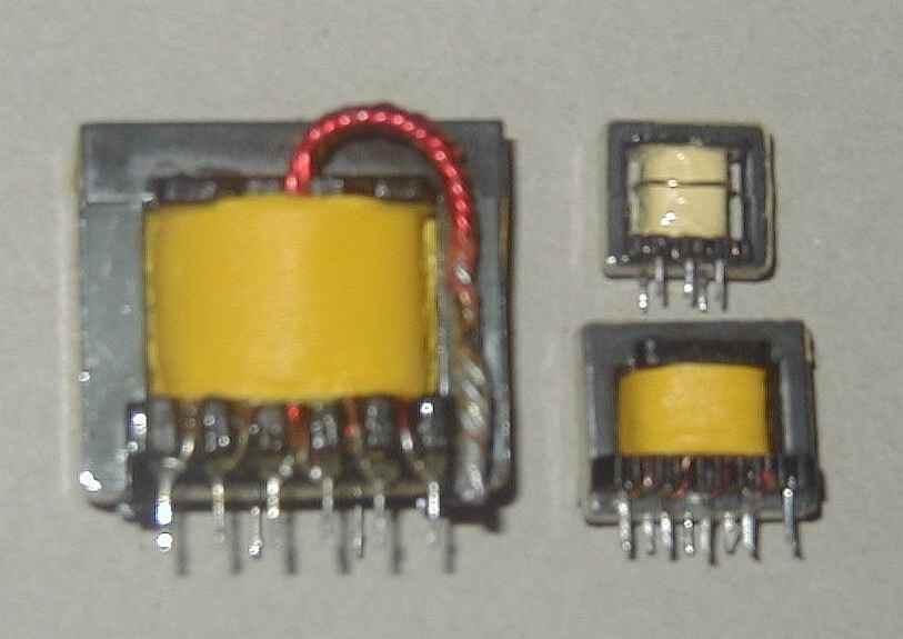
Magnetic components from a PC power supply
The magnetic components of AT-style PC power supplies don't vary much. They are usually designed for a switching frequency of 25... 40 kHz and a power output of 200... 240 W. The transformers on the S.M.P.S circuit boards are to be found often in either a small, or a somewhat larger size. I am not able to say, whether the larger size brings more power or if it is only an older design. [Note: the larger size is usually found in flyback supplies. ja] For the new power supply I preferred the larger transformers because they have more space available for additional turns in all three transformers. The smaller transformers are completely filled with copper and insulation, and are therefore only marginally suitable for modification.
Fig. 1: Transformers from the PC power supply
Mains rectifier and filter
This circuit section is uncomplicated. The common-mode choke Dr1 (mains filter) is followed by a NTC resistor for limiting the inrush current. Its resistance amounts to 5 ohms cold, and after few minutes the warm resistance is less than one ohm. The 230 Vac rectifier is generously specified at 4 A, so no cooling is necessary. The values of capacitors of C3 and C4 is determined by the allowable ripple voltage Ubr, and the number of mains-voltage half-cycles to be bridged [i.e., 'hold-up' time required]. For Ubr = 25 V and zero half-cycles, two 470 uF capacitors in series are sufficient. This specification applies to maximum load during low mains-voltage Umin = 230 Vac - 15%
Fig. 2: Filter, rectifier and power switches
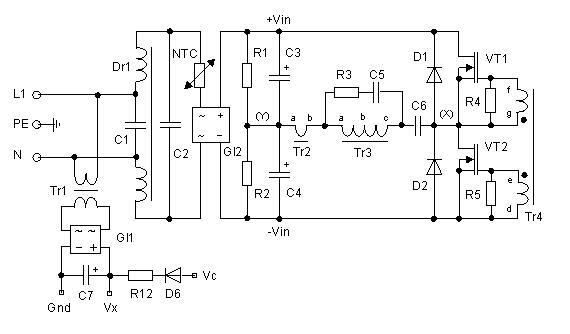
Power switches
FET power switches were used for their short rise and fall times and the easy, component-saving driver circuit. If one is content with switching times of 100 ns, a small driver transformer and two gate resistors suffice for driving the FETs. Unfortunately, there's no way to avoid re-winding the transformer secondary, which is needed to supply the proper gate voltages. The single turn and 2 x 8 turns must be removed from transformer Tr4. Instead of this, wind 2 x 16 turns (bifilar). A winding ratio of 16 : 26 and a 20 V control signal from IC1 provides the FETs' gates with 10 V of drive, enough to achieve the FETs' specified Ron of 0,75 ohms and thus very small conduction losses. Dynamic (switching) losses at 50 kHz are negligible with the before-mentioned switching times. The PWM IC drives enough current to switch the FETs on and off quickly. Increasing the switching frequency from the original 33 kHz (PC power supply) to 50 kHz (new power supply) allows the transformer to more energy. You can't, however, arbitrarily increase frequency with a given transformer; the transformer is only usable over a certain frequency range. Experiments showed the transformer can cope with a factor of 1.5 without problems (overheating).
Control circuit
After switching the 230 Vac mains voltage on, an auxiliary voltage from the small 50 Hz transformer Tr1 powers the PWM controller SG3525. The error amplifier in the SG3525 compares a portion of the 13,8 output voltage (actual value) with the internal +5,1 V reference voltage (set value) and forms from it an error voltage for the pulse width modulator. The modulator sends alternate control pulses via its two outputs to the transformer Tr4. The pulse duration is inversely proportional to the error voltage. Increased loading on the +13.8 V output makes for wider pulses; lighter loading causes narrower pulses. The switching frequency of the power switches is 50 kHz. For higher frequencies the FETs are usable, but not the magnetic components salvaged from the PC power supply. The oscillator frequency is determined by the components attached to pin 5 and 6. R14 determines the dead time, which is absolutely necessary to avoid simultaneous conduction of the two switching transistors. Since they lacking the storage time limitation of bipolar transistors, a very small value can be set for the the new FETs switches. With 1 us deadtime and 20 us period duration--50KHz--the FETs can theoretically conduct 95 % of the time and thus deliver energy to the output. Soft-start capacitor C13 charges after power-on, producing a soft-start with narrow pulses initially, then wider control pulses afterwards. Terminal (a) of the driver transformer Tr4 remains free. Just one half (26 t) of the primary turns (b - c) and the 16 turns of the secondary winding are sufficient to provide the necessary ratio of 0,6.
Fig. 3: PWM control and monitoring
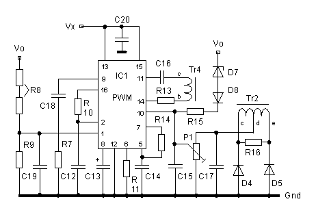
Monitoring functions
Two protection circuits are included in the new power supply. The transformer Tr2 is used as current detector and produces a voltage across R16 that's proportional to the current flow through the power switches. If the voltage at the shutdown pin 10 exceeds the limit value adjustable with P1, the control IC switches off immediately, restarting after a short duration. The reason for this is usually excessive current at the secondary side of the power transformer, either caused by a short-circuit, or an overload to the output. The load and the circuit itself are likewise protected from overvoltage at the Vo output. The SG3525 switches off at Vo > 15 V. Note: Both protection circuits are ineffective if the slider of P1 is adjusted to Gnd potential.
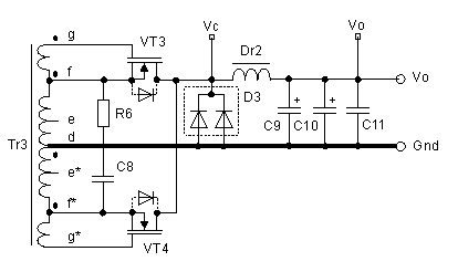
Synchronous rectifier
A rectifier made with fast recovery diodes loses up to 17 W at 18 A output current. Even with a 30 A / 45 V Schottky diode, the losses are still 12 W. This is the supply's greatest single loss, exceeding the losses at the mains rectifier, power switches, transformers, and output choke combined.
An improvement brings here a semi synchronous rectifier with two low impedance power FETs. FETs with a low Ron of e.g. 15 mOhm have only a voltage drop of 0,3 V at 18 A during the conduction phase. Good Schottky diodes are rated at 0,6 V. In the literature, however, with push-pull topology, such circuits are advised against because the choke Dr2's current will flow backwards through the FETs' parasitic body diodes while they're in the 'off' state. High switching losses result due to the storage charge of the body diodes, which has to be removed first before/during the transition to the normal operation. This loss destroys the benefits achieved during the conduction phase.
The following circuit avoids this disadvantage, since the body diodes never conduct. Schottky free-wheeling diode D3 has a substantially smaller forward voltage Uf than the FET's body diode, and so takes over choke Dr2's current. D3 has minimal storage charge, so switching is extremely fast and losses are low. As a test, D3 was removed. The FETs' heat sink warmed up thereupon by around +10 °C, even though the body diode of the IRFZ44 used has a very good trr (reverse recovery time) of 47 ns.
With a typical duty cycle of 57 % the loss in the two FETs together is 3.6 W. The free wheeling diode D3 conducts for the remaining time, dissipating 4.6 W. Losses below 8.2 W can only be achieved by replacing free-wheeling diode D3 with a FET. Since driving this FET is more complex than for VT3 and VT4, I did without this. A second complication is that with mains undervoltage or high output current, the switch-on time of VT3/4 rises, but not the switch-on time of D3.
Fig. 4: Synchronous rectifier
Construction and alignment
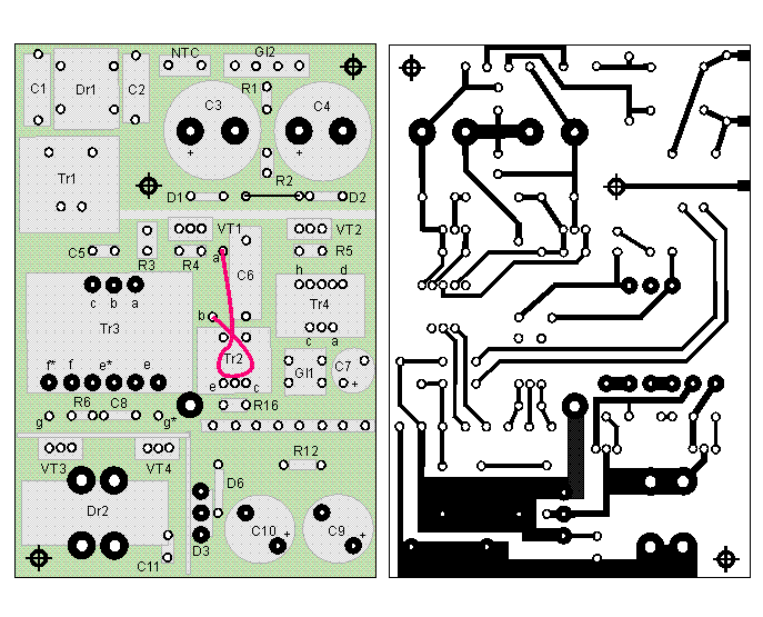
The power supply uses an 82 x 122 mm glass-epoxy circuit board. Other materials are not suitable, as the board must be able to carry relatively heavy components and realize high-current copper tracks. The components for regulation and monitoring are mounted on a small strip board. Sorry, but I was too lazy to design a PCB layout for this circuit part.
Fig.5: PCB layout (1:1) and assembly
For the interconnection of the components for regulation and monitoring a 40 x 45 mm small strip-board is sufficient. The copper tracks (pink) are to be removed in the indicated places. A wood or a metal drill with a diameter from 3 to 4 mm is suited to this task. Jumpers are drawn as broken lines. (They're easily forgotten during assembly! The same applies to the horizontal ground-potential bar within the upper area of the strip-board that distributes Gnd potential onto the vertical copper tracks.
Fig.6: View of the strip-board soldering side (2:1)
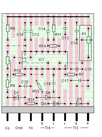
Fig. 7: View of the strip-board component side (2:1)
Transformers
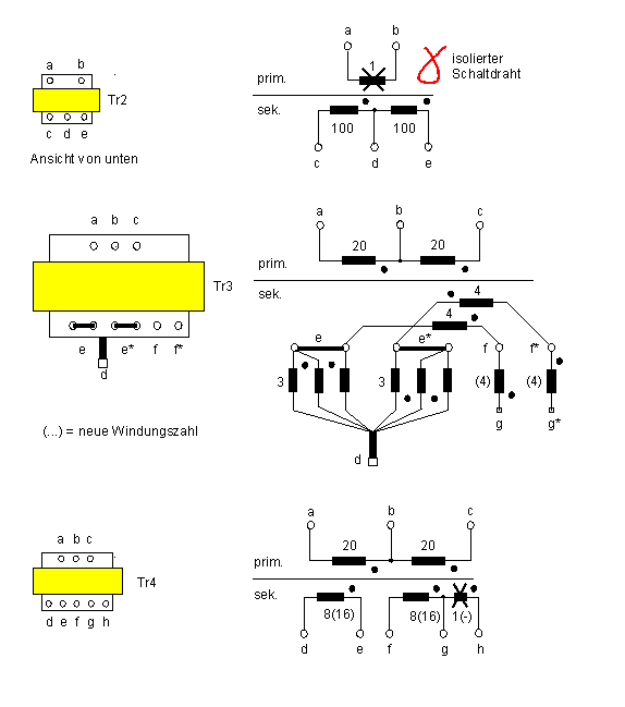
The following drawing shows the transformers stripped from a PC switching power supply. The data were determined as best as possible by measurements, counting turns, and calculations.
Before using the transformers, it must to be confirmed that the size, number of layers, wire size, number of turns and phasing correspond to the specification in the drawing and the photos. If there's any doubt about whether your transformers match these specs, the transformers should not be used.
Fig. 8: PC transformers and modifications
Heat sinks
The heat sinks are nothing special, manufactured from an approx. 1 mm thick aluminum plate. VT1 and VT2 are to be fastened isolated on the first heat sink. The FETs must not have a electrical connection to each other, or to the heat sink. With proper, professional assembly of the transistors [e.g., insulated from the heatsink], touching the heat sink isn't dangerous. On the secondary side it is somewhat simpler. VT3, VT4 and D3 carry no dangerous voltage, and need thus no isolation. Because of the FETs case and the Schottky diodes case have the same potential, there is no problem with mounting all three components directly onto the second heat sink. Be sure, however, that there's no electrical connection between the heat sink itself and the power supply housing or electrical components.
Fig.9: Heat sink drawings
Parts list (1)
Resistors, capacitors and semiconductors
| Parts No. | Value |
| R1, 2 | 120 kOhm, 0,5 W |
| R3 | 100 Ohm , 2 W |
| R4, 5, 9 | 1 kOhm |
| R6 | 10 Ohm, 2 W |
| R7, 10 | 10 kOhm |
| R8 | 1,5 KOhm + 150 Ohm |
| R11 | 5,6 kOhm |
| R12, 13, 14 | 47 Ohm |
| R15, 16 | 150 Ohm |
| P1 | 10 kOhm trimming pot, 10 turns |
| NTC | Heissleiter, 5 Ohm at 25 °C |
| C1, 2 | 0,1 uF 250 Vac |
| C3, 4 | 470 uF 200 V, 22 x 36 mm (diam. , H) |
| C5, 15 | 2,2 nF |
| C6 | 1 uF, 250 Vac |
| C9, 10 | 2200 uF, 35 V low ESR, 16 x 34 mm (Diam., H) |
| C7 | 100 µF, 35 V |
| C8, C20 | 10 nF |
| C11,12 | 0,22 µF |
| C13 | 10 uF, 25 V |
| C14 | 2,2 nF Styroflex |
| C16 | 2,2 uF |
| C17, 18, 19 | 0,047 uF |
| D1, 2 | PXPR1507 etc. fast 200 V / 1A diode |
| D3 | MBR3045, 30 A / 45 V Schottky diode |
| D4, 5, 6 | BAT 46 |
| D7 | Zener diode, 13 V / 0,5 W |
| D8 | 1N4148 |
| VT1, 2 | IRF730 |
| VT3, 4 | IRFZ44N |
| IC1 | SG3525A |
| Gl1 | Rectifier bridge, dual in-line B40C800 DIP |
| Gl2 | Rectifier bridge 400 V / 4 A |
Parts list (2)
Transformers, chokes and miscellaneous
| Parts No. | Value |
| Tr1 | 0,5 W print transformer EE20/10, 15 Vac at 34 mA,
24 x 32 mm (Reichelt/Conrad) |
| Tr2 | 16 x 15 x 5 mm (W,H,D) |
| 1 turn. prim. |
| 2x 100 turns sec. |
| Tr3 | 40 x 35 x 12 mm (W,H,D) e.g. Tokin 25812 or. 25801 |
| 2x 20 turns prim. (L = 7 mH between a <=> c) |
| 2x (3 + 4) turns sec. (L = 200 uH between d <=> f or d* <=> f*) |
| 2x 4 turns sec. auxiliary winding for driving VT3/4 |
| Tr4 | 22 x 19 x 6 mm (W,H,D) |
| 2x 26 turns. prim. |
| 2x 16 turns. sec. |
| Dr1 | current compensated 2A mains voltage choke |
| Dr2 | 20 uH, T26-106 (yel. / white), 16 turns. 2x 1 mm Cu wires in parallel |
| better Magnetics Kool 259-77934-A7, 20 turns. 2x1 mm Cu wires in parallel |
| Additional mains filter | general purpose 230 V / 2 A |
| Si | 3,15 AT fuse, slow blow |
| PS | Two pole mains switch |
| Miscellaneous | PCB, heat sinks, isolation material, heat sink compounder etc. |
The grey marked cells indicate the components, which can be scavenged from a PC power supply. The electrical data must be compared before using them, and the indicated modifications have to be made.
Testing the power supply
I urgently advise against immediate connection to 230 Vac. Testing of the new power supply should take place in several test phases for safety reasons, and for the avoidance of component destruction. The high voltage causes an immediate destruction of the components in the case of an error in the circuit.
Warning: Check temperature of components only if the mains voltage is switched off.
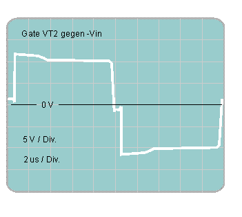
Phase 1:The first test applies to the PWM-IC and the power switch control. For running the PWM-IC, connect a 24Vdc lab power supply to Gnd and the positive plate of C7 (Vx). After switching on, the IC generates sharply rising and falling control pulses with maximum pulse duration at the output pins 11 and 14. With an oscilloscope, signals measured at the gate of VT2 (VT1) should look like the one shown in figure 9. It's very important that the signals have the indicated shape, voltage and frequency. Further, the signals at the gates of VT1 and VT2 should be opposite in phase (otherwise, both FETs would conduct at the same time, producing a short-circuit later, when applying supply voltage).
Fig. 9: VT2 (VT1) gate-source voltage
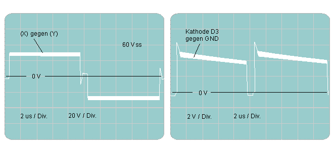
Phase 2: Now, connect three car light bulbs (12 V / 21 W) to the 13,8 V output terminals. A 48 V / 1 A mains transformer feeds the S.M.P.S. via the L1 and N terminal with a galvanically isolated Ac voltage. The + 24 Vdc lab supply is still connected during this test. 60 Vdc at C3 / C4 is in Europe defined as a non-dangerous voltage. At this voltage the switching transistors can start operating, allowing one to perform testing without danger. For measurements with a dual-channel oscilloscope Gnd from the secondary section has to be connected temporarily to the (Y) test point of the primary section with a wire link. The bulbs glow at Vout = 4,3 Vdc if everything is right. Rectification is performed by the FETs body diodes only, because the VT3 and VT4 gate-source voltage is not high enough to switch on the FET. The PWM controller tries to produce 13,8 V at the output at maximum pulse duration / duty cycle. The latter cannot be successful due to the low 60 Vdc input voltage and the present transformer ratio.
Fig. 10: Voltage at test point (X) against (Y) und cathode D3 against Gnd
Phase 3:If everything is all right so far, one can proceed with the exciting test at 230 Vac. The laboratory power supply, the 48 V transformer, the measuring instruments and all provisional cable links attached for the test etc. must obviously be removed. The three car bulbs are further needed as a load and for the functional checks. If after applying of the 230 Vac mains voltage the lamps light up brightly, the output voltage is 13.8 V, and no undefined noises or smells are noticeable, one has won the first round. If an error has slipped past the pre-testing undetected, the two switching transistors and copper tracks say “good-bye” with a more or less loud bang. With 5,7 A, the duty cycle D = tp / T = 5 us / 10 us is approximately 50 %.
Phase 4: For the following load test a dummy load is needed that can handle up to 300 W. Because such high power resistors are expensive, and not just laying about in the junk box, I instead took a 50 m a ring installation cable (3 x 1.5 mm2) . An individual wire has a resistance of 0.6 ohms and can dissipate the mentioned watts without problems. Depending on interconnection of the three wires, load resistances of 0,6 / 1,2 and 1.8 ohms are realizable. By the ampmeter impedance, including the appropriate measuring wires positioned in series, the resistance value increases by approx. 0.1 ohms. At Vo = 13,8 V the following table indicates the power output Po and the current Io as a function of the loading
| Rl [Ohm] | car bulbs | Io [A] | Po [W] |
| - / - | 1x 12 V / 21 W | 1,9 | 26 |
| - / - | 2x 12 V / 21 W | 3,8 | 52 |
| - / - | 3x 12 V / 21 W | 5,7 | 78 |
| 1,8 + 0,1 | - / - | 7,26 | 100 |
| 1,2 + 0,1 | - / - | 10,6 | 146 |
| 1,2 + 0,1 | 2x 12V / 21 W | 10,6 + 3,8 | 198 |
| 1,2 + 0,1 | 3x 12V / 21 W | 10,6 + 5,7 | 224 |
| 0,6 + 0,1 | - / - | 19,7 | 270 |
Additional measures for RFI noise reduction
Experience during the PC power supply modification have shown that the on-board filtering is insufficient for amateur radio applications. A pre-fabbed general purpose mains filter and a home made Pi filter direct to the 13,8 V output are used for improved RF noise reduction. To maintain control loop stability, the PI filter is outside the control loop, so its voltage drop isn't eliminated by the supply's regulation. Output voltage changes of several tens of millivolts under load changes have no importance for running a 100 W transceiver. The additional filters have to be mounted inside the S.M.P.S. case very close to the cable inlet and outlet.
Fig. 11: External components for RF noise reduction
Operation experiences
Up to 10 A continuous output current, or operation with 50 % ESD and 18 A peak current are possible without a fan if sufficient natural air flow is present and the ambient temperature does not exceed 30 °C. A small CPU fan (40 x 40 mm) should be used for more than 10 A continuous current. The heatsink surface is not large enough to keep the FETs junction temperature below the limit value ( Tj < 100 °C). With a CPU fan the heat sink temperature remains below 28 °C (Tu = 20 °C). The following table shows the measured and calculated power dissipation Pv of the basic components at 250 W output power.
| Abbr. | Parts | Pv [W] |
| Gl2, Dr1 | Mains rectifier and filter | 2,5 |
| VT1 | Switching transistors | 4,0 |
| VT2 | 4,0 |
| R3 / C5 | Snubbers | 1,5 |
| Tr3 |


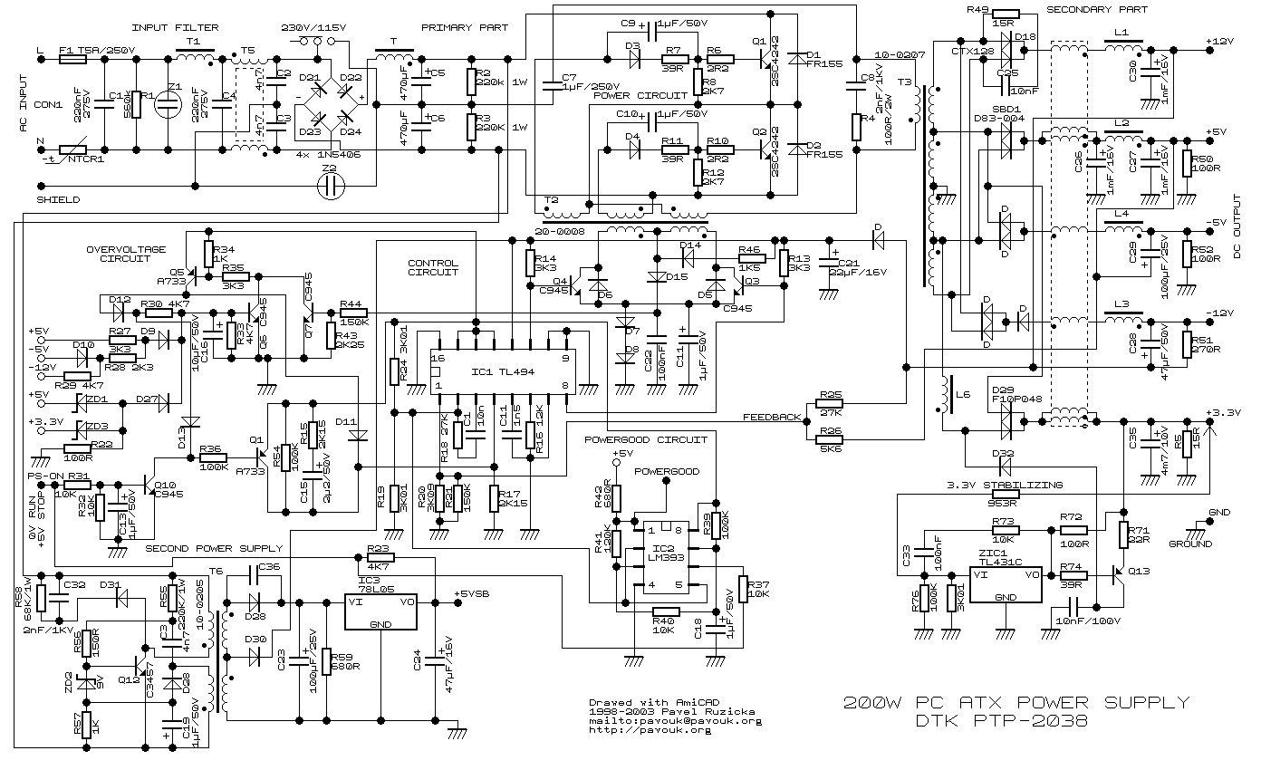 Line voltage goes through input filter circuit (C1, R1, T1, C4, T5) to the bridge rectifier. When voltage is switched from 230V to 115V, then rectifier works like a doubler. Varistors Z1 and Z2 have overvoltage protect function on the line input.


